
Artificial intelligence may be transforming the world, but behind every breakthrough lies a less visible challenge — moving staggering volumes of data between processors without slowing everything down. That’s precisely the problem Hyderabad-based LightSpeed Photonics has set out to solve. Building the future of data bandwidth-intensive applications, the deep-tech startup is replacing conventional copper wires and bulky transceivers with compact, solderable optical interconnects that enable faster, low-power, high-bandwidth data transfer for network cards, switches, and computing. Its patented optical solutions, designed to sit closer to the chip, are 20 times smaller, consume three to five times less power, and deliver three times the bandwidth of conventional transceivers, while enabling significant reductions in power consumption and PCB footprint. In an exclusive chat with CE, Dr Rohin Y, founder-CEO, of LightSpeed Photonics explains how a six-year vision to eliminate data bottlenecks is translating into compact, energy-efficient photonic solutions with global ambitions.
Excerpts
What inspired the founding of LightSpeed Photonics?
LightSpeed Photonics was founded with the belief that computing demand would surge dramatically. While AI is a major driver, high-performance computing (HPC) extends far beyond it, powering applications such as genomics, drug discovery, weather prediction, and scientific research.
High-performance computing requires processing enormous amounts of data in a structured manner. AI is essentially intelligence and algorithms applied to this data, but even before AI, big-data processing depended on moving vast amounts of information between multiple processors. We foresaw that this data movement would become the biggest bottleneck because complex problems can no longer be solved by a single computer — they require multiple GPUs and processors working together. Solving that bottleneck became our mission.
While AI will drive commercial adoption, the technology will eventually extend into automotive, consumer, and industrial applications. Traditional optical pluggables connect data centres or enable fibre-to-home internet. Our focus, however, has always been accelerating computing inside data centres by enabling GPUs and compute servers to exchange data at extremely high speeds. We started this deep-tech photonics company with the vision of building the future of computing through high-speed optical interconnects.
For those unfamiliar with photonics, how would you explain the problem LightSpeed Photonics is solving?
Earlier systems relied on electrical interconnects because data transfer speeds were relatively modest. The limitation with electricity is that electrons interact with their surroundings, creating losses. Light is the fastest medium in the universe and travels with minimal loss, making photonics the fastest and most efficient way to transfer data.
In the AI era, this need has shifted from long-distance communication, such as transatlantic cables or fibre-to-home, to communication between processors inside and across servers. A ChatGPT query may involve only a few kilobytes of text, but behind the scenes, AI models process terabytes or even petabytes of data exchanged between processors. Recommendation engines used by platforms like YouTube and Netflix work similarly, analysing enormous datasets to generate personalised suggestions.
As AI workloads grow, traditional copper-based interconnects are no longer sufficient. Modern data centres must maximise compute density while moving massive amounts of data in and out of chips. Solving this bandwidth challenge is the primary role of photonics in the AI era.
Your optical interconnects are said to be 20 times smaller and consume significantly less power while delivering higher bandwidth than existing solutions. What technological breakthrough made this possible?
The breakthrough comes from heterogeneous integration — bringing together multiple materials and technologies into a single system that functions seamlessly. It combines physics, electronics, materials engineering, optics, firmware, and software into one integrated architecture.
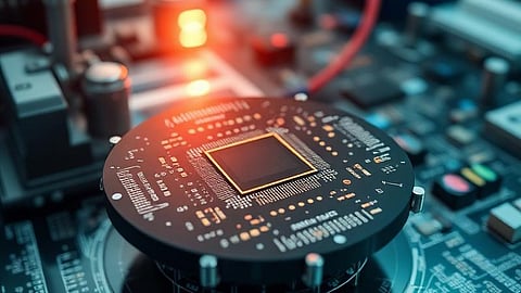
Our chip is about the size of a SIM card yet transfers 400 gigabytes of data per second. Unlike a SIM card, it doesn’t store data; it transfers it between an optical fibre and a nearby compute chip.
A traditional pluggable transceiver is much larger. Our solution integrates four lasers, four lenses, optical fibres, electronics, and different substrate materials into a compact package. These different components must operate as a single system. Our interdisciplinary expertise, supported by global technology partnerships, forms the core of our competitive advantage. Compared to similar technologies worldwide, we are also able to build this solution at a fraction of the cost through frugal engineering.
Why did LightSpeed Photonics choose to focus on near-packaged optics instead of conventional pluggable transceivers?
The decision is largely architectural. Conventional pluggable transceivers sit at the edge of a server, far from the processor. As data rates increase, electrical signals weaken over distance, making it impossible to transmit them efficiently to the edge.
A simple analogy is Wi-Fi versus mobile networks. Wi-Fi offers higher speeds but only over short distances, while mobile signals cover larger areas with lower bandwidth. Similarly, very high-speed signals must stay close to the processor, making compact optical interconnects essential.
It’s also a real-estate problem. Delivering ten times the bandwidth within the same physical space requires much smaller components positioned closer together. Compact interconnects also reduce the overall footprint of AI data centres by allowing both computing and networking hardware to occupy less space.
How much of an impact can LightSpeed Photonics’ technology have on reducing operational costs and energy usage at scale?
Historically, networking consumed only a small share of data centre power because data centres primarily stored information. Today, AI data centres focus on computation, with GPUs and cooling systems accounting for most energy consumption.
As more processors are packed into smaller spaces, networking requirements have increased dramatically. Networking power consumption has risen from around 10% of a data centre’s total energy usage to nearly 25%, and is expected to reach 40%. It has become one of the largest contributors to operational costs.
Our technology reduces networking power consumption by five to seven times compared to conventional pluggable transceivers, offering significant energy savings for next-generation AI data centres.
What has been the biggest hurdle in taking LightSpeed Photonics from the R&D stage to industry adoption?
The biggest challenge has been building the right technology partnerships. Early on, a strong track record and technical credibility helped us gain the attention of industry leaders and secure support for developing the product.
As we move towards commercialisation, the challenges shift to securing long-term commitments from major customers while demonstrating manufacturability, reliability, and production readiness. Hardware differs from software because once deployed, customers expect support for five to ten years or longer. Trust, collaboration, and long-term commitment are therefore essential.
Our journey has been about evolving from an unknown company into a recognised player capable of delivering scalable, manufacturable technology. As we approach commercialisation, these efforts are beginning to pay off.
How closely are you working with chip makers, OEMs, and data centre operators to ensure your technologies integrate seamlessly into existing infrastructure?
Chip makers typically create reference designs that recommend components for next-generation hardware, which OEMs then use to develop systems. In some cases, data centre operators drive the process by requesting new architectures from OEMs or chip makers.
We work closely with all three groups. The first step is getting our technology included in reference designs. From there, customers conduct pilots by integrating our technology into their own hardware for testing. Once performance is validated, they evaluate manufacturing facilities, reliability, and production readiness before moving towards commercial deployment. We are currently preparing for this phase so that today’s pilot projects become tomorrow’s large-volume manufacturing opportunities.
How is LightSpeed Photonics positioning itself to support the next generation of AI-driven data centres and high-performance computing?
We are well positioned to play a significant role in next-generation AI infrastructure. Our collaborations with chip makers and OEMs focus on developing future architectures, including disaggregated systems and high-bandwidth connectivity solutions that will underpin AI data centres.
Over the next five years, we expect the industry to transition from pilot projects to small-volume manufacturing and eventually to large-scale production. Because we anticipated these requirements years in advance, we believe we are well positioned to capture this opportunity. Hardware cannot be developed only when demand arrives — it must be ready beforehand.
Where do you envision LightSpeed Photonics in the coming years?
We aim to become a major global player in photonics, not just in India or Southeast Asia. Over the next five years, we plan to scale our design capabilities, technology, partnerships, manufacturing, and support infrastructure to serve customers worldwide.
Today, we are the only company of our kind in this region. While we may still be relatively small, the industry is at an inflection point. As photonics becomes central to AI infrastructure, we believe the next five years will be transformational for both the technology and our company.
