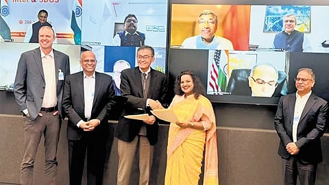

BHUBANESWAR: In a big push to Odisha’s vision for emerging as the semiconductor hub of India, the state government on Friday signed an MoU with the Intel Corporation and 3D Glass Solutions Inc. USA at Santa Clara in California for establishing an advanced packaging glass core substrate manufacturing facility here.
The project, with an estimated investment of around USD 3.3 billion, will be one of the largest high-technology manufacturing investments in the country. The facility is proposed to be located in the Bhubaneswar-Khurda region.
Official sources said that the project is planned to be implemented in phases over a period of five to six years. It will focus on producing advanced packaging glass core substrates, high-density interconnect substrates and associated semiconductor technologies, with Intel supporting technology know-how and process expertise.
It is expected to generate over 1,800 direct high-skilled employment opportunities while creating significant indirect employment across the broader manufacturing and technology ecosystem.
Chief Minister Mohan Charan Majhi, Union minister for Electronics and IT Ashwini Vaishnaw, Intel Corporation CEO Lip-Bu Tan and other officials witnessed the signing of the MoU. Addressing the function virtually, the chief minister said the signing of the MoU is the beginning of a new chapter in Odisha’s growth story.
“This initiative goes beyond semiconductor manufacturing. It is about creating a future where Odisha becomes a globally competitive destination for advanced technologies, innovation, AI infrastructure, data centres and digital transformation,” he said.
Stating that the government’s vision is to build a vibrant ecosystem that creates world-class opportunities for the youth, the chief minister said the new project will firmly place Odisha on the global semiconductor map.
“This is a transformational, generational opportunity that will accelerate economic growth, strengthen India’s technological self-reliance and position Odisha at the forefront of the global digital economy,” he added.
Majhi said aligned with Odisha Vision-2036 and India’s vision of Atmanirbhar Bharat, this initiative reinforces the state’s commitment to developing a globally competitive semiconductor, electronics, AI, and digital infrastructure ecosystem that will serve both national priorities and global markets.
Vaishnaw termed the agreement a landmark in the country’s efforts to develop the entire ecosystem of semiconductor manufacturing. He said that the entry of firms like Applied Materials Inc., Lam Research, Tokyo Electron Ltd., Merck Electronics and signing of the MoU between Tata Electronics and Dutch multinational ASML, is a recognition of the Centre’s efforts in the semiconductor sector and the trust the industry places in India.
Chief secretary Anu Garg, who was present at the signing of the MoU, said it marked a transformative step in Odisha’s journey towards becoming a key player in advanced semiconductor and electronics manufacturing. “With strong policy support, skilled talent and integrated infrastructure, Odisha is ready to contribute meaningfully to India’s semiconductor ambitions,” she said.
Babu Mandava, CEO of 3D Glass Solutions, said this initiative has the potential to establish India as a key global hub for advanced glass substrates and semiconductor packaging, supporting high-growth sectors such as artificial intelligence, high-performance computing and next-generation electronics.
Executive vice-president and general manager of Intel Foundry Naga Chandrasekaran said “Intel Foundry is proud to collaborate with 3DGS in exploring this opportunity with the government of Odisha.”
